Showing posts with label PCB-Design. Show all posts

Thursday, May 16, 2024

PCB Etching Compensation For Manufacturing

Introduction to Etching Compensation

One critical step in the PCB manufacturing process is etching, where unwanted copper is removed to form the desired circuit patterns. However, during etching, factors such as chemical reactions and process variations can cause deviations from the intended design. This is where etching compensation comes into play.

PCB Etching


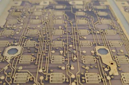
Etching compensation involves adjusting the dimensions of the artwork to account for material removal during the etching process. By pre-emptively altering the trace widths and spacing on the design files, manufacturers can ensure the final product closely matches the intended specifications. This compensation is crucial for maintaining the electrical performance and reliability of the PCB.

The importance of etching compensation cannot be overstated. Precise control over the trace widths and spacing is essential for achieving the desired electrical characteristics, such as impedance and signal integrity. Without proper compensation, the etched traces could end up too narrow or too wide, leading to potential failures in the electronic device.

In this blog, we will explore why etching compensation is necessary, its impact on impedance, the relevant IPC standards, how manufacturers handle compensation for high-speed PCB and high-frequency PCB, and best practices to achieve optimal results.

Why Etching Compensation is Necessary from a PCB Manufacturing Perspective

The etching process involves several steps, including coating the PCB with a photoresist, exposing it to a pattern, developing the exposed resist, and finally etching away the unprotected copper. Despite advancements in manufacturing technology, the etching process is still subject to various factors that can affect the precision of the trace widths and spacing. These factors include:

  • Chemical concentration: Variations in the concentration of the etching solution can lead to uneven material removal.
  • Temperature fluctuations: Changes in temperature can affect the rate of chemical reactions, causing inconsistencies in etching.
  • Process duration: The time the PCB is exposed to the etching solution can impact the amount of copper removed.
  • Equipment calibration: Inaccuracies in the calibration of etching equipment can lead to deviations from the desired dimensions.

These challenges make it difficult to achieve the precise trace widths required for modern PCBs. Without etching compensation, the final traces may be too thin, leading to increased resistance, reduced current-carrying capacity, and potential overheating. Conversely, traces that are too wide can result in crosstalk, signal interference, and compromised circuit performance.

Etching compensation addresses these issues by adjusting the original artwork to account for the expected material removal. By doing so, manufacturers can produce PCBs that meet the stringent requirements of electronic devices, ensuring reliable operation and long-term durability.

Will Etching Compensation Affect Impedance Output?

Impedance is a critical parameter in PCB design, especially for high-frequency and high-speed applications. It refers to the resistance to the flow of alternating current (AC) in a circuit and is influenced by the trace width, trace thickness, and the dielectric properties of the PCB material. Maintaining the correct impedance control is essential for signal integrity and minimizing signal loss.

Etching compensation directly impacts impedance because it alters the trace widths. If the compensation is not done correctly, the resulting traces may not match the intended impedance, leading to signal integrity issues. For instance, if the traces are narrower than designed, the impedance will be higher, causing signal reflections and potential data errors. Conversely, wider traces result in lower impedance, which can also degrade signal quality.

Manufacturers address this by carefully calculating the amount of compensation needed to achieve the desired impedance. This involves:

  • Pre-compensation calculations: Determining the expected material removal and adjusting the trace widths accordingly.
  • Test coupons: Creating test structures on the PCB that can be measured to verify the actual impedance after etching.
  • Iterative adjustments: Fine-tuning the compensation parameters based on the test results to ensure the final traces meet the impedance requirements.

By implementing these strategies, PCB manufacturers can ensure that etching compensation does not adversely affect impedance, maintaining the signal integrity and performance of the PCB.

IPC Etching Tolerance from Original Artwork

The IPC sets the standards for PCB design and manufacturing to ensure consistency, reliability, and quality across the industry. One such standard is IPC-6012, which specifies the performance and qualification requirements for rigid PCBs. Within this standard, there are guidelines for etching tolerance, which refer to the allowable deviations from the original artwork dimensions.

According to IPC-6012, the etching tolerance typically ranges from ±10% to ±20% of the trace width. This means that if a trace is designed to be 10 mils wide, the actual width after etching should be within 9 to 11 mils for a ±10% tolerance. Adhering to these standards is crucial for ensuring that the PCB meets the design specifications and performs as intended.

Manufacturers use these standards as a benchmark for their etching processes. By following the IPC guidelines, they can produce PCBs that are consistent in quality and performance, reducing the risk of failures and ensuring customer satisfaction.

How Factories Control Their Etching Compensation for High-Speed or High-Frequency PCBs

High-speed and high-frequency PCBs present unique challenges for etching compensation. These PCBs require tighter control over trace widths and spacing to maintain signal integrity and minimize losses. Factories employ several techniques to achieve the necessary precision:

  • Advanced photolithography: Using high-resolution photomasks and precise exposure equipment to create accurate patterns on the PCB.
  • Automated process control: Implementing automated systems to monitor and adjust the etching process in real-time, ensuring consistent results.
  • Regular calibration: Frequently calibrating equipment to maintain accuracy and prevent deviations from the desired dimensions.
  • Statistical process control (SPC): Using statistical methods to analyze process data and identify trends or anomalies, allowing for proactive adjustments.

By leveraging these techniques, manufacturers can effectively control etching compensation for high-speed and high-frequency PCBs, ensuring that the final products meet the stringent performance requirements of modern electronic devices.

Best Practices for Etching Compensation

Achieving optimal results in etching compensation requires collaboration between PCB designers and manufacturers. Here are some best practices to consider:

  • Design for manufacturability (DFM): Incorporate etching compensation into the design phase, considering the manufacturing capabilities and limitations.
  • Use of simulation tools: Utilize software tools to simulate the etching process and predict the necessary compensation adjustments.
  • Regular communication: Maintain open lines of communication between designers and manufacturers to address any issues or changes in the design or process.
  • Continuous improvement: Implement a feedback loop to review the performance of the etching process and make continuous improvements.

By following these best practices, both designers and manufacturers can ensure that etching compensation is effectively implemented, resulting in high-quality PCBs that meet the demands of modern electronic devices.

Sunday, May 12, 2024

Flex Circuit Board: Key Insights & Strategies

Flex circuit boards, also known as flexible PCBs, These versatile components are essential in modern devices where space and weight are limited, providing outstanding flexibility and durability compared to traditional rigid PCBs. This technology enables designers to push the boundaries of electronics design, creating more compact, lightweight, and complex devices that meet the evolving demands of today's tech-driven world.

Flex Circuit Board


In this blog, we will delve into the intricacies of flexible PCBs, examining the best materials for use, particularly focusing on polyimide and its optimal thickness for various applications. We'll explore why certain surface finishes are preferred and discuss stackup considerations that can significantly influence both performance and cost. Our discussion will also cover the durability of these boards, the critical IPC standards governing their quality, challenges faced during production, cost-effective manufacturing strategies, and the environmental impacts associated with their production.

Through this comprehensive guide, electronics engineers, PCB designers, and supply chain professionals will gain insights into making informed decisions about flexible PCBs, ensuring they choose the right materials, designs, and manufacturing processes to meet their project requirements effectively and efficiently.

Flexible PCB Materials and Design Considerations


A: Materials Used in Flex PCBs

Flexible PCBs require materials that can withstand extreme bending and folding without compromising the integrity of the circuit. The choice of materials not only affects the performance but also the manufacturability and longevity of the flex circuit. Among various materials available, polyimide stands out due to its exceptional thermal stability, chemical resistance, and flexibility.

Polyimide Flex PCBs:

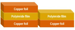
Polyimide
Polyimide (PI) is the material of choice for most flexible PCB applications due to its robust performance in harsh environments. It is known for its excellent heat resistance — capable of operating in temperatures as high as 400 degrees Celsius — and its impressive mechanical properties. These characteristics make polyimide ideal for dynamic or high-temperature applications, including aerospace, automotive, and consumer electronics.

Thickness Variations:

  • 25um Polyimide: Often used in very flexible, high-density applications where the space is at a premium. It offers superior flexibility, making it ideal for intricate designs that require tight bending capabilities.
  • 75um Polyimide: This thickness is a balanced option, providing a good mix of flexibility and mechanical strength, suitable for both dynamic and static applications.
  • 100um Polyimide: Opted for projects requiring increased mechanical strength and durability. While less flexible than its thinner counterparts, it is beneficial in applications where minimal bending is involved.

The thickness choice directly impacts the cost—the thicker the polyimide, the more expensive the PCB and reducing of bending ratio. Designers must balance cost with performance requirements, considering how the board will be used in the final product.

B: Flexible PCB Stackup and Design

Stackup Configuration:

Flex Stack Up
The stackup — the arrangement of insulating layers and conductive circuits in a PCB — is crucial in determining the board's overall performance. In flexible PCBs, the stackup must be designed to maximize the flexural endurance without sacrificing electrical integrity.

Single-Layer Flex: Consists of a single conductor layer on a flexible dielectric film, ideal for static applications where minimal bending occurs.

Double-Layer Flex: Two conductive layers with an insulating layer in-between, suitable for dynamic applications where the board may experience frequent bending.

Multilayer Flex: Multiple conductive layers separated by insulating materials, used in highly complex circuits requiring robust electrical performance and minimal space.

C: Impedance Control Techniques:

Flex Impedance

Controlling impedance is critical in flexible PCBs to ensure reliable signal integrity across the circuit. Techniques include:

  • Precise control of trace width and spacing.
  • Consistent dielectric material properties.
  • Use of shielding layers to reduce external noise interference.


Cost Considerations:

Design complexity and material choice significantly impact the cost. For instance, multilayer flex PCB are more expensive due to their complex manufacturing processes. Designers must consider the trade-offs between performance, durability, and cost to optimize the board for both functionality and budget.

Flex PCB Durability and Standards


A. Durability Factors of Flexible PCBs

Durability is a paramount concern in the design and manufacture of flexible PCBs. The very flexibility that makes these boards so valuable also introduces unique challenges in ensuring they can withstand repeated bending and harsh operating conditions.

Key Durability Factors:

  • Material Selection: As previously discussed, polyimide is favored for its high thermal stability and mechanical endurance. The choice of adhesive material, which bonds the conductive layers to the substrate, also plays a critical role. It must maintain its adhesive properties under thermal stress and repeated flexing.
  • Copper Type: The type of copper used affects flexibility and durability. Rolled annealed (RA) copper is softer and more malleable, making it better suited for applications where the PCB will undergo extensive bending. Electrodeposited (ED) copper, though stiffer, is often used in applications requiring finer line widths.
  • Through-Hole Plating: Reliable through-hole plating techniques are crucial for maintaining electrical continuity, especially in flex areas where mechanical stress is concentrated. Poor plating can lead to failures in electrical connections under stress.

Testing Procedures:

To ensure the durability of flexible PCBs, several testing procedures are employed:

  • Bend Testing: Simulates the bending and flexing that the board will endure during its operational life.
  • Thermal Testing: Assesses how well the board withstands temperature extremes and thermal cycling.
  • Pull and Peel Tests: Measure the strength of adhesion between layers and the robustness of the surface mount components.

These tests help manufacturers identify potential failure points and improve board design and material selection to enhance durability.

B. IPC Standards for Flex Circuits

The IPC 6013 standard governs the performance and quality requirements for flexible printed boards. Adherence to this standard is crucial for ensuring that flexible PCBs meet the rigorous demands of various applications.

Key Aspects of IPC 6013:

  • Class 1, 2, and 3 Requirements: Defines the criteria for different levels of performance, from general electronic products (Class 1) to high-reliability military and aerospace applications (Class 3).
  • Material and Conductor Thickness: Specifies acceptable materials and minimum conductor thicknesses based on the application’s complexity and reliability needs.
  • Testing and Acceptance Criteria: Outlines the required tests for validating the integrity and functionality of flex circuits under different operational stresses.

Compliance with these standards not only ensures product reliability but also enhances the manufacturer's credibility in the market, making it a crucial consideration for designers and engineers in the industry.

Challenges in Flexible PCB Production

Flexible PCB manufacturing involves distinct challenges that differ significantly from those encountered in traditional rigid PCB production. Addressing these issues requires specialized techniques, innovative materials, and a deep understanding of flex circuit design intricacies.

Common Production Challenges:

  • Handling and Assembly: Due to their inherent flexibility, handling flex circuits without causing damage or deformation can be challenging. Automated assembly processes need to be carefully calibrated to avoid excessive stress on the boards.
  • Alignment and Registration: During multilayer flex PCB fabrication, maintaining precise alignment of the layers is critical, especially given the material's tendency to stretch and contract. Misalignment can lead to functional failures and reduced reliability.
  • Miniaturization: As devices become smaller, flex PCBs need to accommodate tighter bends and more compact configurations, which can complicate the manufacturing process and increase the risk of mechanical stress failures.

Surface Finish Options:

Choosing the right surface finish is crucial for enhancing the solderability and reliability of flex circuits. The surface finish protects the copper from oxidation and provides a solderable surface when connecting components.

  • ENIG (Electroless Nickel Immersion Gold): Provides a flat surface and is suitable for fine-pitch components, making it a popular choice for high-density flex circuits.
  • OSP (Organic Solderability Preservatives): A cost-effective option that offers good solderability but may not be as robust as other finishes for repeated flexing.
  • Immersion Tin or Silver: These finishes offer excellent solderability and maintain a flat surface, but they can be prone to tarnishing and are less durable under thermal stress.

Technological Solutions:

To overcome these challenges, manufacturers employ various advanced techniques:

  • Laser Direct Imaging (LDI): Improves alignment accuracy by allowing for precise and adaptable pattern creation, essential for the high-density requirements of modern flex circuits.
  • Automated Optical Inspection (AOI): Ensures quality control by detecting and correcting defects early in the manufacturing process.
  • Use of Stiffeners: Adding stiffeners in strategic areas can provide additional support during assembly and use, reducing stress on vulnerable parts of the flex circuit.

Cost-Effective Solutions for Flex PCB Manufacturing


Achieving cost-effectiveness in flexible PCB production is essential for manufacturers looking to offer competitive pricing while maintaining high-quality standards. Implementing strategic approaches can significantly reduce costs without compromising the performance and reliability of the final product.

Strategies to Reduce Manufacturing Costs:


  • Design Optimization: By optimizing the design for manufacturability, manufacturers can reduce waste and increase production efficiency. This involves minimizing the use of wide traces and large pad sizes when not necessary, and strategically placing components to reduce the total number of layers needed.
  • Material Selection: Choosing the right materials from the start can lead to significant cost savings. For example, selecting a slightly thicker polyimide may increase material costs but can reduce processing steps and improve yield by enhancing durability.
  • Volume Production: Leveraging economies of scale by producing larger volumes can decrease the unit cost significantly. Planning production runs to maximize panel utilization also reduces waste and lowers the cost per unit.

Case Studies and Examples:


A notable example involves a manufacturer who redesigned their flex circuit layout to optimize space utilization, resulting in a 20% reduction in material costs and a 15% decrease in production time.
Another case saw the implementation of automated testing procedures, which reduced labor costs and increased throughput, improving overall efficiency and reducing scrap rates by minimizing human error.

Influence of Design Complexity on Costs:


  • Complexity of the Design: Higher complexity generally leads to increased costs due to more material layers and additional processing steps. Simplifying the design where possible can lead to substantial cost savings.
  • Technology Integration: Advanced manufacturing technologies such as laser etching and automated placement machines can initially increase capital costs but pay off in the long run by improving accuracy, reducing waste, and speeding up production.

Choosing the Right Flex Circuit Manufacturer

Selecting a manufacturer for flexible PCBs is a critical decision that can significantly affect the quality, reliability, and overall success of your project. It requires careful consideration of various factors to ensure that the chosen supplier can meet your specific needs and standards.

Criteria for Choosing a Manufacturer:

Certifications and Compliance: Look for advanced manufacturers that adhere to industry standards and hold relevant certifications, such as ISO 9001 for quality management systems and IPC 6013 for specific flex PCB requirements. These certifications are indicators of the manufacturer’s commitment to quality and consistency.

Manufacturing Capabilities: Assess the technological capabilities of the manufacturer, including their ability to produce various flex PCB types, such as single-sided, double-sided, and multilayer flex circuits. Check for advanced manufacturing processes that can handle the specific requirements of your design, such as precision laser cutting and automated optical inspection systems.

Experience and Reputation: Consider the manufacturer’s track record and industry reputation. Look at reviews, case studies, and testimonials from other customers, particularly those in similar industries or with similar application requirements. Experience in handling complex and high-reliability flex circuits can be a significant advantage.

Supply Chain Robustness: Evaluate the robustness of the manufacturer’s supply chain, including material sourcing, lead times, and their ability to handle fluctuations in demand. A reliable supply chain is crucial for meeting project timelines and avoiding costly delays.

Cost Structure: While cost should not be the sole deciding factor, it is important to understand the pricing structure of the manufacturer. Ensure that the cost aligns with the budget constraints of your project without compromising the quality or performance of the flex circuits.

Support and Communication: Good communication is key to any successful partnership. Choose a manufacturer who provides clear and consistent communication throughout the design and production process. Support services such as design assistance, prototyping, and after-sales support are valuable services that can greatly enhance the manufacturing experience.

Tips on Vetting Potential Suppliers:

  • Request Samples: Obtain samples of the manufacturer’s previous work to evaluate the quality and compatibility with your needs.
  • Visit the Facility: If possible, visit the manufacturing facility to get a firsthand look at their operations and processes.
  • Ask for References: Speak to current or past customers to gain insights into their experiences with the manufacturer.

Environmental Impact of Flexible PCB Manufacturing

The manufacturing of flexible PCBs, like many industrial processes, has a significant environmental footprint. Awareness and efforts towards minimizing this impact are crucial, as they not only comply with regulatory standards but also appeal to the growing consumer and corporate demand for environmentally responsible products.

Key Environmental Concerns:

  • Use of Hazardous Chemicals: The production of flex PCBs involves various chemicals, particularly in the etching and plating processes, which can be harmful if not managed properly. Chemicals such as copper sulfate used in plating and various solvents in cleaning processes need careful handling and disposal.
  • Waste Production: Flex PCB manufacturing generates solid and liquid waste, including metal scraps, used chemicals, and excess polyimide material. Proper waste management procedures are essential to minimize environmental harm.
  • Energy Consumption: The production process is energy-intensive, especially in high-precision manufacturing tasks like laser cutting and automated inspection. Optimizing energy use and sourcing renewable energy can significantly reduce the carbon footprint.

Sustainable Practices in Manufacturing:

  • Recycling and Reuse: Implementing recycling programs for metal scraps and other recyclable materials can significantly reduce waste. Some advanced manufacturers are exploring ways to reuse polyimide and other materials in new production cycles.
  • Lean Manufacturing: Adopting lean manufacturing principles can help reduce waste and improve efficiency. This includes minimizing unused materials, optimizing production processes to use less energy, and reducing the overall waste generated.
  • Eco-friendly Material Alternatives: Research into alternative materials that have a lower environmental impact than traditional polyimide is ongoing. Bio-based and recyclable polymers are being considered as potential substitutes that can provide similar performance with less environmental burden.

Future Trends and Innovations:

  • Technological Advancements: Advances in manufacturing technology that increase yield and efficiency while reducing waste and energy consumption are likely to continue. Automation and improved process control can lead to more sustainable manufacturing practices.
  • Regulatory Compliance: Compliance with environmental regulations is not just about avoiding penalties; it's also about leading the industry towards more sustainable practices. Manufacturers who proactively exceed compliance requirements can improve their market position and brand reputation.
  • Consumer Demand: As consumers and businesses become more environmentally conscious, they demand greener products. Manufacturers that can demonstrate sustainable manufacturing practices and the environmental friendliness of their products have a competitive edge.

Conclusion

Throughout this detailed exploration of flexible PCBs, we have uncovered the complexities and innovations driving this crucial component of modern electronics. From the selection of materials like polyimide with varying thicknesses tailored to specific applications, to the intricate designs of stackup configurations ensuring optimal performance, flexible PCBs are at the forefront of technological advancement.

We delved into the crucial aspects of durability and adherence to IPC standards, highlighting how these factors ensure reliability and consistency in flex circuit board manufacturing. The challenges faced in production, particularly in handling, alignment, and miniaturization, were also discussed, alongside technological solutions that enhance quality and efficiency.

Cost-effective manufacturing strategies are vital for maintaining competitiveness in the industry. By optimizing design, selecting appropriate materials, and scaling production, manufacturers can significantly reduce costs without sacrificing quality. Selecting the right manufacturing partner, one that aligns with technical requirements and values, is essential for the successful implementation of flex PCBs in any project.

Moreover, we addressed the environmental impacts associated with flexible PCB manufacturing. Emphasizing sustainable practices, from waste management to the adoption of eco-friendly materials, is not just a regulatory compliance issue but a critical component of future industry standards. As the demand for greener products increases, manufacturers who lead in sustainability will likely lead the market.

Looking Forward:

The future of flexible PCB technology is bright, with ongoing advancements in materials science, manufacturing processes, and environmental sustainability set to further revolutionize this field. As electronic devices continue to evolve towards more compact and complex designs, the flexibility, durability, and efficiency offered by flex PCBs will become increasingly crucial.

For engineers, designers, and decision-makers in the electronics industry, understanding these aspects of flexible PCBs is essential. It ensures not only the functionality and reliability of their products but also their competitiveness and compliance with evolving environmental standards. As we move forward, the continuous innovation and improvement in flexible PCB manufacturing will undoubtedly open new horizons for electronic applications, making what seems complex today, standard tomorrow.
Wednesday, May 8, 2024

Designing Feasible Multi-Layer PCB Stackup

This posts delves into the specifics of PCB stack-up design with a focus on Design for Manufacturing (DFM) for 4, 6, and 8 layer PCBs. It explores how thoughtful design can significantly influence manufacturing efficiency, cost-effectiveness, and product reliability. By understanding the subtleties of stack-up design, electronics engineers and PCB designers can optimize their boards for both performance and manufacturing costs, navigating the complexities of PCB material choicesimpedance control, and layer count implications with greater confidence.

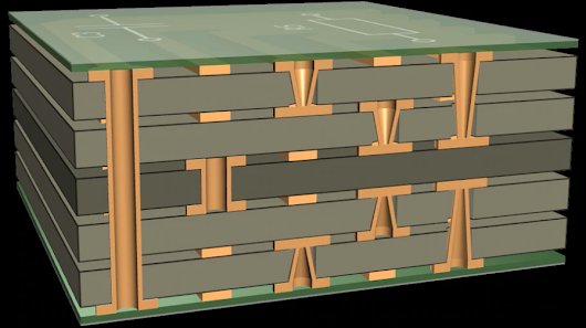
Multiple Layer PCB Stackup


Understanding The Multilayer PCB Stack-Up 

What is PCB Stack-Up?

PCB stack-up refers to the arrangement of copper layers and insulating materials in a printed circuit board. This structure is crucial because it determines the electrical properties, thermal management, and mechanical stability of the PCB. A well-designed stack-up can enhance signal integrity, reduce electromagnetic interference (EMI), and manage power distribution more effectively.

Common Configurations

PCB stack-ups vary in complexity from simple single-layer boards to intricate multi-layer designs. The most common multi-layer configurations are:

  • 4-Layer PCB Stackup: Typically consists of two signal layers and two planes (power and ground). This configuration is ideal for moderately complex circuits, offering a balance between cost and performance.
  • 6-Layer PCB Stackup: Provides additional layers for improved shielding and routing space for complex circuits, usually involving four signal layers interspersed with power and ground planes.
  • 8-Layer PCB Stackup: Ideal for advanced applications with high-density interconnects, providing ample layering for signal integrity and minimal cross-talk.

Each configuration has its specific uses, benefits, and design considerations, which will be explored in detail in the following sections.

DFM Design for PCB Stack-Up


Overview of DFM in PCB Manufacturing

Design for Manufacturing (DFM) is a critical practice in PCB design that ensures the manufacturability of the board while minimizing cost and maximizing efficiency. It involves designing PCBs in such a way that they are easy to manufacture without requiring excessive engineering changes during the production phase.

Designing a 4-Layer PCB Stack-Up

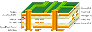
A 4-layer PCB is often the choice for designs that need more than a double-layer board but do not require the complexity of a 6 or 8-layer board. The typical stack-up configuration is:

4 Layer PCB Stackup

Top layer (Signal)
Internal plane (Ground)
Internal plane (Power)
Bottom layer (Signal)

This setup provides good EMC performance with minimal cost. By using only one core and two sheets of prepreg, a 4-layer board can be manufactured cost-effectively, balancing performance with production simplicity.

Designing a 6-Layer PCB Stack-Up

Moving to a 6-layer PCB allows for greater separation of power and ground planes from the signal layers, reducing EMI and improving signal integrity. The common stack-up might look like:

6 Layer PCB Stackup
Top layer (Signal)
Ground
Power
Signal
Bottom layer (Signal)
Signal


This configuration uses two cores and three sheets of prepreg, which increases the cost but provides better performance for more complex circuits.

Designing an 8-Layer PCB Stack-Up

An 8-layer PCB is used in high-density designs where additional layers are necessary for multiple power and ground layers or for intricate routing requirements. The typical configuration might include:


Top layer (Signal)
Ground
Signal
Signal
Ground
Signal
Bottom layer (Signal)
Signal

This arrangement, using three cores and four sheets of prepreg, significantly increases the material costs but is essential for achieving the desired electrical performance in advanced circuit electronic systems.

The next sections will build upon these configurations, discussing their impact on costs, the implications of design choices on PCB warpage, and more.

Cost Implications of Stack-Up Design


Cost Analysis of PCB Layers and Material Use

The cost of a PCB largely depends on the number of layers, the type and quantity of materials used (such as core and prepreg), and the complexity of the manufacturing processes involved. Here's how different stack-up designs impact the overall cost:

  • 4-Layer PCB: Utilizing one core and two sheets of prepreg, a 4-layer PCB is generally the most cost-effective option for multi-layer boards. The use of a single core helps keep material costs down while providing sufficient functionality for many applications.
  • 6-Layer PCB: This design typically uses two cores and three sheets of prepreg, increasing the material costs due to the additional core. The complexity of alignment during layering also adds to the manufacturing cost but offers better performance for complex circuits.
  • 8-Layer PCB: With three cores and four sheets of prepreg, the 8-layer PCB is the most expensive among the three due to the high material usage and the intricate manufacturing process required to ensure layer alignment and reliability.

Practical Cost-Saving Strategies

To optimize the cost of manufacturing PCBs without compromising quality, designers can employ several strategies:

  • Optimize layer count to match the complexity of the application.
  • Choose materials judiciously based on performance requirements and cost.
  • Design for manufacturability to reduce waste and streamline production processes. 
  • Adheres to the standard number of Core material (Typically a 4-layer stackup utilizes one core, a 6-layer stackup uses two cores, and an 8-layer stackup incorporates three cores. The use of more cores increases the cost of the PCB.)

Impact of Stack-Up Design on Warpage


Understanding PCB Warpage

Warpage in PCBs occurs due to the thermal mismatch between different materials and uneven cooling rates, which can lead to bending or twisting of the board. This deformation can affect the reliability and assembly of the PCB, especially during the reflow soldering process.

How Stack-Up Design Influences Warpage

Symmetrical Stack-Up: One of the most effective ways to reduce warpage is to design a symmetrical stack-up. This involves arranging the core and prepreg layers in a balanced manner so that the thermal expansion on one side is countered by the other.
Material Choice and Thickness: Using materials with similar thermal expansion properties and managing the thickness of prepreg and core layers can also help minimize warpage.

Tips for Reducing Warpage in PCB Design

  • Maintain a balanced and symmetrical layer structure.
  • Select materials with compatible thermal properties.
  • Design with uniform copper density across all layers to prevent uneven heating and cooling.

Impedance Control in PCB Stack-Up 


Significance of Impedance Control

Impedance control is crucial in PCB design to ensure signal integrity, particularly in high-speed applications. The stack-up configuration plays a key role in managing impedance by determining the electromagnetic characteristics of the board.

How Impedance Requirements Affect PCB Stack-Up

Layer Arrangement: The positioning of signal and ground layers significantly affects the impedance characteristics. For instance, closely coupling signal layers with ground planes can help achieve more controlled impedance.
Material Properties: The dielectric constant of the materials used also influences impedance. Designers need to select the right core and prepreg materials that provide the desired dielectric properties.

Strategies for Achieving Desired Impedance

  • Use consistent spacing between layers to maintain uniform impedance across the board.
  • Select materials with stable dielectric constants under varying environmental conditions.
  • Implement careful routing and placement of components to avoid impedance mismatches.

Material Selection for PCB Stack-Up


Types of Prepreg and Core Materials

In PCB manufacturing, the choice of prepreg and core materials is vital for determining the board's thermal and electrical performance.

Common Core Materials: FR-4 is the most widely used material due to its good mechanical and electrical properties at a reasonable cost. For higher performance, materials like polyimide are used in more demanding applications.
Common Prepreg Materials: Prepreg materials, typically made of woven glass fabric impregnated with epoxy resin, are selected based on their resin content, glass transition temperature, and dielectric properties.

Selection Criteria for Prepreg and Core Materials

  • Consider thermal stability, dielectric constant, and mechanical strength.
  • Balance performance requirements with cost constraints.

Deciding on Prepreg Adhesive Thickness 


Role of Prepreg Adhesive Thickness in PCB Stack-Up

The thickness of the prepreg adhesive layer is crucial for ensuring good lamination bonding between the layers of a PCB, which affects both the mechanical integrity and the thermal performance of the board.

Guidelines for Selecting Adhesive Thickness

Thermal and Mechanical Requirements: The selected thickness should provide adequate bonding while supporting the board's thermal and mechanical demands.
Manufacturing Constraints: Consider the limitations and capabilities of the PCB manufacturing process when selecting the adhesive thickness to ensure a reliable production process.

Conclusion: Optimizing PCB Design for Performance and Manufacturing

The intricate process of PCB stack-up design plays a fundamental role in determining the functionality, reliability, and manufacturability of electronic devices. As we have explored, each decision from the number of layers to the choice of materials impacts not just the electrical performance of the PCB but also its cost and susceptibility to issues like warpage.

For electronics engineers and PCB designers, achieving an optimal balance between complexity and cost efficiency requires a deep understanding of DFM principles and a strategic approach to material selection and layer configuration. By carefully designing a 4, 6, or 8 layer stack-up, designers can meet specific impedance requirements, minimize warpage, and ensure robust performance in the final product.

In conclusion, while the technical challenges of designing efficient PCB stack-ups are significant, the benefits of a well-considered design are profound. It not only enhances the product's performance but also streamlines the manufacturing process, reducing costs and improving yield rates. As technology advances, the principles of effective PCB design remain crucial in driving innovations and ensuring the success of electronic products in increasingly competitive markets.

Monday, May 6, 2024

Key Trends in PCB Design: Automation, Collaboration, and Simulation

Today's PCB designers face the dual challenges of escalating system demands and the push for faster time-to-market. To navigate these challenges, significant trends have emerged in PCB design: Automation, Collaboration, and Simulation. This blog post explores these trends and their implications for the future of PCB design, providing insights into cutting-edge tools and techniques that are shaping this dynamic field.

Circuit Board Design


Automation in PCB Design

Automation in PCB design is revolutionizing the way circuits are conceived, designed, and tested for a complex circuit board design such as ATE Boards, Probe Cards, Load Boards, BIB Boards and so on.... Automated tools leverage algorithms to optimize board layouts, route complex interconnections, and perform intricate checks on designs to ensure compliance with electrical and mechanical specifications. Key areas where automation is making a profound impact include:

Schematic Design Automation: Tools like OrCAD and Altium Designer automate the creation of schematics, reducing the likelihood of human error and ensuring design integrity from the start.

Auto-Routing: Advanced auto-routing features are integral to tools such as Eagle and KiCAD, which significantly reduce the time required to design complex multilayer boards.

Design Rule Checking (DRC): Automated DRC systems rigorously check each aspect of the PCB design against predefined rules, ensuring that the final product is manufacturable without costly revisions.

The adoption of automation not only enhances efficiency but also enables designers to handle increasingly complex designs that would be impractical to manage manually.

Collaboration in PCB Design

As projects become more complex involving multidisciplinary teams, Collaborative PCB Design has become essential. Cloud-based platforms and tools facilitate real-time collaboration among team members dispersed across different geographies. This collaborative approach ensures that all stakeholders, including design engineers, manufacturing teams, and supply chain partners, are aligned, leading to:

  • Enhanced Design Accuracy: Shared workspaces and synchronized design environments reduce miscommunications and errors, leading to higher accuracy and fewer revisions.
  • Reduced Time to Market: With real-time collaboration, changes can be made quickly and efficiently, significantly cutting down the development cycle.
  • Increased Innovation: Collaborative environments foster innovation by integrating diverse expertise and perspectives into the design process.

Tools like Autodesk Fusion 360 and Altium 365 are at the forefront, offering integrated environments where design, testing, and production teams can work seamlessly together.

Simulation in PCB Design

Simulation technologies have grown indispensable in modern PCB design, allowing designers to predict and rectify potential issues early in the design process. By simulating different aspects of the PCB, designers can:

Electromagnetic Compatibility (EMC) Simulation: Tools like Ansys HFSS simulate electromagnetic fields in PCBs, predicting electromagnetic interference and compatibility issues.

Thermal Simulation: Simulations help predict heat build-up and dissipation in circuit boards, which is crucial for high-power or densely packed devices.

Signal Integrity Analysis: High-speed designs often suffer from signal integrity issues; simulation tools can model and analyze signal behavior to mitigate problems like crosstalk and noise.

These simulations are vital for ensuring the reliability and functionality of PCBs in real-world applications.

The Future of PCB Design

Looking ahead, the future of PCB design is poised to be more integrated and intelligent, with advancements in AI and machine learning leading the charge. Predictive design tools, smarter automation, and more robust simulation capabilities will further streamline the design process. Moreover, the integration of IoT and real-time data analytics will enable more dynamic and responsive PCB systems.

Conclusion

The ongoing evolution in PCB design through automation, collaboration, and simulation is equipping designers to meet current and future challenges. As electronic devices continue to grow in complexity and functionality, the tools and techniques at the disposal of PCB designers will not just keep pace but often drive the innovations. Understanding and leveraging these trends is crucial for any PCB designer aiming to remain at the cutting edge of PCB technology.

This exploration not only underscores the importance of embracing new technologies but also highlights the exciting possibilities that lie ahead in the realm of PCB design. As we look to the future, the role of sophisticated design tools and Collaborative Platforms will undoubtedly become more central in transforming ideas into reality, ensuring that the field of PCB design continues to innovate and inspire.

Saturday, May 4, 2024

Flex PCB Solder Mask vs. FPC Coverlay

 Flex Solder Mask vs Coverlay

Flexible circuit board (flex PCB) are a cornerstone in modern electronics due to their adaptability and efficiency in complex designs. Key to their fabrication and functionality are the protective layers applied over the conductive traces: flex PCB solder mask and Flexible Printed Circuit (FPC) Coverlay. This post delves into the distinctions, advantages, and disadvantages of these materials, alongside the minimum capability for dam size, all from a top PCB manufacturer perspective.

Flex Solder Mask and FPC Coverlay - The Difference?

Flex PCB Solder Mask:

  • Definition: Similar to rigid PCBs, a solder mask on a flex PCB is a thin protective layer applied directly over the copper traces, but formulated to withstand bending and flexing.
  • Thickness: The thickness typically ranges from 10 to 30 microns, allowing for a very tight fit to the circuit pattern.
  • Application Process: Typically applied through screen printing or photolithographic techniques, flex PCB solder masks are less bulky than coverlay, allowing for finer detail in smaller spaces.

FPC Coverlay:

  • Definition: FPC coverlay consist of a polyimide film laminated with an adhesive layer, offering robust protection against environmental factors and mechanical stress.
  • Thickness: Generally, the combined thickness of the polyimide and adhesive layers ranges from 50 to 200 microns, significantly thicker than solder masks.
  • Application Process: The coverlay is cut to size and shape, then laminated onto the PCB using heat and pressure to bond securely over the circuitry.

Flex Solder Mask and FPC Coverlay - Pros & Cons?

The Pros of Flex PCB Solder Mask:

  • Cost-Effectiveness: Generally cheaper than coverlay due to simpler application processes.
  • Ease of Application: Can be applied quickly in the same manner as solder masks on rigid PCBs, which reduces manufacturing time.
  • Environmental Resistance: Offers good resistance against humidity and contaminants.
  • Dam Size: The minimum dam size for a solder mask is typically around 100 microns, making it suitable for circuits where space conservation is crucial.

The Cons of Flex PCB Solder Mask:

  • Reduced Flexibility: Less suitable for applications requiring significant bending, as it can crack under repeated flexing.
  • Limited Use in High-Density Areas: May not be suitable for very dense flex circuits as it can complicate the soldering process.

The Pros of FPC Coverlay:

  • Enhanced Durability: Provides superior mechanical protection, which is crucial for high-reliability applications and reducing the risk of circuit failure.
  • Superior Flexibility: Designed to withstand continuous bending and twisting without degradation.

The Cons of FPC Coverlay:

  • Higher Cost: The material and lamination process are more expensive than the simple application of solder masks.
  • Complex Application Process: Requires precise alignment and lamination, which can increase production times.
  • Dam Size: The minimum dam size for coverlay can be as large as 300 microns due to the thickness of the materials used, which might impact the compactness of the PCB design.

IPC Standards and Specifications For Flex PCB:

  • IPC Standards for Flex PCB Solder Mask: The IPC-SM-840C classification sets the standards for durability, adhesion, and thickness of solder masks, including those used on flex PCBs. These standards ensure that the solder mask can withstand the intended operational environment without failing.
  • IPC Standards for FPC Coverlay: IPC-4204A outlines the requirements for flexible metal-clad dielectrics used in the fabrication of flexible printed circuitry. It includes standards for material properties, adhesive performance, and dimensional stability of coverlay, ensuring that they meet the high demands of flex circuit applications.

Stringent standards set by the IPC For Flex PCB:

  • IPC Class 2: Focuses on general industrial applications where extended life is required, but uninterrupted service is not critical.
  • IPC Class 3: Pertains to high-reliability electronics where continuous performance is essential, such as in medical or military applications.

PCB Manufacturing Perspective: Best Practices

From a PCB manufacturing standpoint, the choice between a solder mask and a coverlay largely depends on the specific requirements of the application:

Bending and Flexing: If the design requires extensive bending, a coverlay is typically preferred due to its enhanced durability and protective qualities.
Fine Feature Applications: For circuits demanding finer detail, a solder mask may be more suitable due to its capability for smaller dam sizes.
Cost and Complexity: Solder masks are generally less expensive and simpler to apply, making them ideal for cost-sensitive projects not requiring high flex.

Conclusion

Choosing between a flex PCB solder mask and an FPC coverlay depends on balancing several factors: the level of flexibility required, environmental conditions, durability needs, and cost constraints. For applications requiring maximal flexibility and durability, coverlay are the preferred choice despite their higher cost and complexity. Conversely, solder masks offer a cost-effective solution for less demanding applications, providing sufficient protection with greater design freedom. As technology evolves, so too will these materials, continuously enhancing the capabilities and applications of flex PCBs in the electronics industry.

Call to Action

Consult with a seasoned PCB Expert to explore the most suitable protection for your flexible circuit boards. For further guidance or to discuss your specific needs, contact us through [Linkedin] or to Discover the Vital Links Technology Difference!

Thursday, May 2, 2024

PCB Surface Finishes: ENIG vs. ENEPIG Explained

ENEPIG vs ENIG


When designing printed circuit boards (PCBs) for various applications in the aerospace, medical, and automotive industries, one of the critical decisions revolves around the choice of surface finish. Two popular types are Electroless Nickel Immersion Gold (ENIG) and Electroless Nickel Electroless Palladium Immersion Gold (ENEPIG). These finishes not only protect the underlying copper from oxidation but also ensure a reliable soldering surface. This article delves into the differences between these finishes, their advantages and disadvantages for your pcb design choice, and general guidelines on when to opt for one over the other.

Understanding PCB Surface Finishes: ENIG vs. ENEPIG

ENIG, is a two-layer metallic coating consisting of an electroless nickel layer capped with a thin layer of immersion gold, which protects the nickel from oxidation. 

ENEPIG, on the other hand, features three layers: an electroless nickel layer, followed by a palladium layer, and finally a thin gold layer. The addition of palladium provides a robust barrier between the nickel and gold layers, enhancing the durability and longevity of the finish.

Pros and Cons of ENIG vs. ENEPIG Surface Finishes

The Pros of ENIG:

  • Uniform Finish: ENIG provides a smooth and flat surface that is ideal for fine-pitch components, helping in avoiding solder bridging.
  • Good Oxidation Resistance: The gold layer protects the nickel from oxidation, ensuring excellent shelf life.
  • RoHS Compliance: ENIG is lead-free and compliant with RoHS regulations, which is essential for electronics intended for the European market.

The Cons of ENIG:

  • Black Pad Issue: One potential risk with ENIG is the black pad phenomenon, where the nickel-phosphorous layer can become brittle and lead to poor solder joints.
  • Cost: ENIG can be more expensive than other finishes due to the use of gold.

The Pros of ENEPIG:

  • Versatile for Multiple Assembly Processes: ENEPIG is suitable for soldering, wire bonding (gold and aluminum), and conductive adhesive bonding, making it incredibly versatile.
  • Eliminates Black Pad Issues: The palladium layer prevents the oxidation of nickel, thereby eliminating the black pad problem associated with ENIG.
  • Long Shelf Life: The robust three-layer protection offers a superior shelf life, crucial for components that may not be immediately used.

The Cons of ENEPIG:

  • Higher Costs: The additional palladium layer increases the cost compared to ENIG.
  • Complexity in Processing: The triple-layer process is more complex to manage, requiring precise control during manufacturing.

When to Use ENEPIG Over ENIG?

ENEPIG is recommended in situations where multiple assembly processes are anticipated for the same PCB or where maximum reliability is required under harsh conditions. It is particularly advantageous in high-reliability fields such as aerospace and medical devices. In contrast, ENIG might be sufficient for less demanding applications but where a flat surface is critical, such as in high-density component assemblies.

Applications in Specific Critical Industries

Aerospace PCBs: ENEPIG is often preferred due to its excellent performance in harsh environments and its ability to support various types of component bonding.

Medical PCBs: The high reliability and non-toxic nature of ENEPIG make it suitable for medical devices, especially those requiring long-term reliability in body or close to body applications.

Automotive PCBs: While ENIG can suffice for general applications, ENEPIG may be chosen for high-reliability needs or where multiple assembly techniques are used.

Challenges and Manufacturing Considerations

The capability to process ENEPIG is not universally available in all PCB manufacturing facilities due to the complex nature of the process and the cost of the materials involved, particularly palladium. Manufacturers need to maintain a highly controlled environment to ensure the quality and consistency of the ENEPIG finish. For projects requiring high reliability, selecting a high quality pcb manufacturer with the capability to provide high-quality ENEPIG finishes is crucial. This often involves evaluating their process controls, quality assurance practices, and the overall reliability of their PCBs.

In conclusion, the choice between ENIG and ENEPIG should be guided by the specific requirements of the application, including the expected environmental conditions, the assembly processes involved, and the need for long-term reliability. Understanding the advantages and limitations of each can help designers make informed decisions that align with the technical requirements and budgetary constraints of their projects.

Wednesday, May 1, 2024

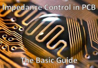
Impedance Control In PCB Basic Guide

Impedance Control In PCB
Impedance control is a critical parameter in the design of printed circuit boards (PCBs), especially for applications involving advanced circuit boards such as high-speed signals and high-frequency environments. Proper impedance control ensures signal integrity and minimizes issues like signal reflection and cross-talk, which are vital for the reliability and performance of electronic systems. This post aims to demystify various aspects of impedance control, from basic concepts to advanced techniques, providing valuable insights for both novice and experienced PCB designers.

Understanding Impedance in PCBs

Trace Impedance refers to the resistance of a PCB signal trace at high frequencies. It is influenced by the trace width, thickness, the dielectric material around it, and the overall layout of the traces. Proper management of trace impedance is essential for maintaining signal integrity across the PCB.

  • Differential Pair Impedance involves two closely spaced traces carrying equal and opposite signals. The key to differential signaling is maintaining consistent impedance to ensure that the signals remain balanced, which is crucial for minimizing electromagnetic interference (EMI) and signal degradation.
  • Single End Impedance Control deals with the impedance of a single trace measured against a reference plane. It's crucial for the design of simpler, less costly PCBs where differential pairs are not feasible.

Material Impact on Impedance Control

The choice of PCB material significantly affects the accuracy of impedance control. Materials like FR-4 are commonly used due to their well-understood characteristics and cost-effectiveness. High-speed and high-frequency applications might require advanced pcb materials such as Rogers or Teflon that provide lower dielectric constants and loss factors, facilitating better impedance control.

PCB Layout for Better Impedance Control

Effective PCB layout is vital for achieving desired impedance levels. Key strategies include:

  • Trace Geometry: Adjusting the width and spacing of traces to match the target impedance.
  • Via Design: Optimizing via structures to minimize impedance discontinuities.
  • Routing Techniques: Using uniform trace routing to avoid impedance variations.

Optimal PCB Stackup Design

Designing an effective stackup is fundamental for multilayer PCBs, where each layer's configuration can impact overall impedance. A well-designed stackup helps in balancing the capacitive and inductive characteristics across the PCB, ensuring consistent impedance.

Impedance Control Techniques

Achieving precise impedance control involves several techniques, especially in multi-layer PCBs:

  • Simulation Tools: Utilizing PCB design software for impedance modeling and simulations.
  • Controlled Dielectric Materials: Selecting materials with consistent dielectric properties.
  • Impedance Testing: Implementing testing protocols to ensure the impedance matches the design specifications.

Challenges in Flexible Circuit Boards

Flexible PCBs pose unique challenges for impedance control due to their varying material properties and dynamic flexing. Designers must consider the mechanical and thermal changes that can affect impedance and employ robust design practices to mitigate these issues.

Tutorial: Implementing Impedance Control

Here's a practical tutorial for implementing impedance control:

  • Design Initiation: Start with clear specifications for impedance requirements.
  • Material Selection: Choose materials based on desired impedance characteristics and application needs.
  • PCB Layout Design: Use design tools to layout traces and vias according to impedance calculations.
  • Simulation and Testing: Run simulations to check for impedance mismatches and make necessary adjustments.

Conclusion

Understanding and implementing impedance control is crucial for designing effective PCBs, especially in high-speed pcb and high-frequency pcb applications. By applying the principles and techniques discussed, designers can ensure their PCBs meet the necessary performance standards.

Tuesday, April 30, 2024

Cost-Effective Rigid Flex PCB Design

Cost Effective Rigid Flex PCB
The adoption of rigid flex PCBs has been steadily increasing due to their ability to integrate the benefits of both rigid and flexible substrates into a single board. However, one critical aspect that engineers and designers often grapple with is the cost associated with these intricate circuit boards. In this technical journal, we delve into a comprehensive cost analysis of rigid flex PCBs, providing invaluable guidelines for optimizing designs, reducing manufacturing expenses, and achieving cost-effective prototypes.

Rigid-Flex PCB Cost Analysis 

Material Selection Guidelines

The choice of material plays a pivotal role in the cost and performance of rigid flex circuits. Common materials include polyimide for the flexible layers due to its excellent thermal stability and durability, and FR-4 for the rigid layers for its cost-effectiveness and mechanical properties. To optimize costs, select materials that meet the minimum required specifications for the application’s thermal, mechanical, and electrical needs. High-performance materials may only be necessary for high-speed or high-temperature applications, so using standard materials where possible can significantly reduce costs.

Panelization Design to Reduce Waste

Panelization involves the arrangement of PCBs on a manufacturing panel in a way that maximizes the number of boards produced while minimizing material waste. Effective panelization is crucial in rigid flex PCB manufacturing due to the expensive materials involved. Designing to standard panel sizes and using nesting techniques, where PCB designs are rotated and placed closely together, can significantly decrease scrap. Moreover, considering the integration of multiple designs on the same panel can further optimize material usage and reduce costs.

Stackup Optimization Strategies

The stackup—the arrangement of copper and insulating layers in a PCB—can also affect costs. An optimized stackup design reduces layer count while ensuring adequate performance, which not only simplifies manufacturing but also cuts costs. Engineers should work closely with manufacturers to determine the most cost-effective stackup that meets the electrical requirements of the application.

Eliminating Unnecessary Manufacturing Requirements

To avoid unnecessary costs, it's crucial to align the PCB design with standard manufacturing capabilities. Custom specifications and tolerances stricter than necessary can lead to higher costs. Standardizing hole sizes, avoiding unusual annular rings or trace widths, and using common via processes can all help reduce costs. Additionally, understanding the manufacturer’s capabilities and designing within these parameters can prevent costly design iterations and tooling charges.

Guidelines for Quick Turn Prototypes

For projects requiring fast turn rigid flex PCBs, it's important to consider how design decisions impact rapid prototyping costs. Utilizing design-for-manufacturing (DFM) principles to ensure that the PCB can be efficiently and quickly produced is key. Simplifying designs for the prototype phase, using materials and processes that are readily available, and maintaining clear communication with the manufacturer can all expedite production without incurring additional costs.

High-Quality Rigid Flex PCB Manufacturers

When it comes to realizing your rigid flex PCB designs with uncompromising quality and cost efficiency, partnering with a reputable manufacturer is paramount. One such industry-leading manufacturer renowned for its commitment to excellence is Vital Links Technology. With a track record of delivering superior rigid flex PCB solutions tailored to the unique needs of electronics engineers and designers, Vital Links stands out for its cutting-edge capabilities, stringent quality control measures, and responsive customer support.

Conclusion

Effective cost management in rigid flex PCB production requires a strategic approach to design and material selection, thoughtful panelization and stackup optimization, and a clear understanding of manufacturing capabilities. By applying these guidelines, electronics engineers and PCB designers can achieve cost-effective solutions without compromising the performance and reliability essential to modern electronic devices. Partnering with skilled manufacturers and leveraging their expertise will further enhance the quality and cost-efficiency of the final products.

Monday, April 22, 2024

Altium vs. KiCad: Choosing the Right PCB Design Software

KiCad vs Altium


In electronics engineering and PCB design, the selection of suitable tools is essential for optimizing efficiency and improving the quality of the final product. With a range of software options available, it can be challenging to decide which tool best fits your needs. Two major contenders in the PCB design software arena are Altium and KiCad. Each offers unique strengths and limitations, appealing to different aspects of the circuit board design process. In this article, we'll delve into a comparison of Altium and KiCad, examine their pros and cons, and explore why someone might opt for professional PCB design services, such as those provided by Vital Links Technology, for manufacturing advanced circuit boards.

Altium Software

Altium


Pros:

  • Comprehensive Integration: Altium is renowned for its robust feature set, integrating schematic capture, PCB layout, and bill of materials management all in one platform. This integration streamlines the design process, making it more efficient.
  • Advanced Capabilities: With features like high-speed design tools, advanced routing technology, and real-time cost estimation, Altium is well-suited for complex projects such as rigid flex pcb & multilayer flex pcb that require meticulous detail and optimization.
  • Strong Support and Resources: Altium offers extensive training materials, tutorials, and a supportive community. Additionally, their customer service is highly responsive, providing assistance when needed.

Cons:

  • Cost: One of the biggest drawbacks of Altium is its cost, which can be prohibitively expensive for hobbyists or smaller companies. The price tag reflects its professional-grade capabilities but can be a barrier for some.
  • Complexity: While its wealth of features is a significant advantage, the learning curve can be steep for beginners or those accustomed to simpler platforms.

Ideal User Profile:

Altium is best suited for professional electronics engineers and organizations that require advanced capabilities and can afford a higher software investment. It's particularly valuable for complex, multi-layered projects where precision and integration of various design components are crucial.

KiCad

kicad


Pros:

  • Cost-Effective: KiCad is open-source and free, making it accessible to everyone from hobbyists to professional designers looking to cut costs.
  • Community and Open Source: Being open-source, KiCad has a supportive community. Users can contribute to its development, which fosters continuous improvement and customization.
  • Cross-Platform Compatibility: KiCad runs on Windows, macOS, and Linux, providing flexibility for users across different operating systems.

Cons:

  • Less Integrated: Unlike Altium, KiCad does not offer the same level of integration or out-of-the-box features. This can result in a need for additional plugins or tools, potentially complicating the design process.
  • Variable User Experience: The user interface and experience can vary significantly depending on the extensions and updates being used. This inconsistency can be a challenge for users expecting a uniform experience.

Ideal User Profile:

KiCad is ideal for individuals, educators, and companies looking for a cost-effective, flexible solution. It is particularly suitable for less complex projects or those where software cost is a significant factor.

Comparing Altium and KiCad

When deciding between Altium and KiCad, consider your specific needs:

Budget: If budget is a constraint, KiCad offers a capable platform without the financial commitment.

Project Complexity: For advanced projects that require detailed management and sophisticated features, Altium is generally more suitable.

Experience Level: Beginners might find KiCad more approachable, though it also lacks some of the automated features that simplify complex designs in Altium.

PCB Design Services and Fabrication: 

For those who require professional PCB design services and fabrication, companies like Vital Links Technology offer comprehensive solutions. These services are particularly beneficial for projects requiring advanced circuit boards, as they combine expertise in PCB design with the capabilities to manufacture high-quality boards. Outsourcing to a professional service can help in ensuring that all aspects of the PCB design are optimized for performance and cost.

Accessing Free PCB Design Software

For beginners or those on a budget, accessing free PCB design software can be invaluable. KiCad, being open-source, is readily available for download and use. Additionally, there are several other free tools available online that can meet basic needs for circuit board design. Websites like EasyEDA and PCBWeb offer free versions that are user-friendly and sufficient for simpler projects.

In conclusion, choosing the right PCB design software depends heavily on specific project requirements, budget constraints, and the level of complexity involved. Both Altium and KiCad have their merits, making them suitable for different types of users and projects. For those looking to combine design and fabrication, turning to specialized services like Vital Links Technology can provide a seamless, professional experience tailored to advanced and complex needs. Whether you opt for the robust features of Altium or the cost-effectiveness of KiCad, understanding your requirements will guide you to the best choice for your PCB design needs.

What's Hot

Newly Published Post

Editor's Choice

Understanding IC Test Boards and Their Types

Integrated Circuit (IC) test boards are critical in ensuring the reliability and performance of electronic components in various application...