Understanding Signal Integrity
Signal integrity is the measure of the quality of an electrical signal as it travels through a circuit. It encompasses various aspects like waveform distortion, noise, timing errors, and impedance mismatches. The goal is to maintain the signal's shape and timing as close to its original form as possible. Signal degradation can result in errors, reduced data rates, and even system failures. As digital systems operate at higher speeds, the margin for error narrows, making signal integrity a paramount concern in PCB design.
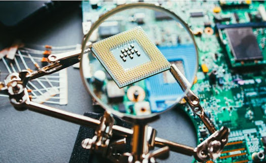
Importance of PCB Layout in Signal Integrity
The PCB layout plays a pivotal role in signal integrity for several reasons. Firstly, the physical routing of traces, placement of components, and the organization of layers in a PCB can affect how signals propagate and interact. Factors such as trace length, width, spacing, and the use of vias can influence signal loss, reflection, and crosstalk. Moreover, the layout determines the electromagnetic compatibility (EMC) of the device, influencing how susceptible it is to external noise and how much interference it may generate for other devices.
Key Considerations for Signal Integrity in PCB Design
Trace Geometry
Trace width, thickness, and length directly impact resistance, capacitance, and inductance, affecting signal speed and integrity. Adhering to controlled impedance standards is crucial for minimizing reflections and ensuring reliable signal transmission.
Layer Stacking
A well-planned PCB layer stackup can provide a consistent reference plane, reduce electromagnetic interference, and facilitate better signal integrity. Strategic placement of signal, ground, and power layers plays a critical role in mitigating cross-talk and reducing signal path loop areas.
Component Placement and Routing
Strategic component placement and thoughtful routing can minimize signal path lengths and reduce potential points of interference. Keeping high-speed signals away from noisy areas and ensuring a clear return path for signals are essential practices.
Decoupling and Power Integrity
Decoupling capacitors are vital for maintaining stable voltage levels and minimizing noise on power planes. Power integrity, closely linked with signal integrity, ensures that all components receive stable, clean power, crucial for the proper functioning of high-speed circuits.
Advanced Techniques for Enhancing Signal Integrity
Differential Pair Routing
Differential pairs are used for transmitting high-speed digital signals, reducing susceptibility to noise and EMI. Proper routing, maintaining consistent spacing and parallelism, is essential for maximizing their effectiveness.
Via Optimization
Vias connect different layers of a PCB but can introduce impedance discontinuities. Optimizing via count, placement, and structure can minimize their impact on signal integrity.
Signal Simulation and Testing
Using software tools for signal integrity simulation and testing can identify potential issues early in the design process. Post-production testing ensures that the PCB meets the required specifications and performance standards.
Real-World Applications and Case Studies
Highlighting real-world scenarios where PCB layout significantly impacted signal integrity can provide valuable insights. Case studies from industries like telecommunications, computing, and aerospace, where signal integrity is critical, can illustrate the consequences of layout decisions and the benefits of adhering to best practices.
Conclusion
The PCB layout is a critical factor influencing signal integrity in electronic devices. As technology advances, the need for meticulous PCB design becomes increasingly vital to ensure functionality, reliability, and performance. Understanding the principles of signal integrity and applying best practices in PCB layout can mitigate issues, enhance device performance, and pave the way for the development of more advanced and reliable electronic systems.