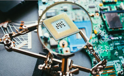
Copper is fundamental in the realm of printed circuit boards (PCBs), Its exceptional electrical conductivity, flexibility, and thermal properties make it indispensable across various applications, from simple electronic devices to complex systems in the automotive and renewable energy sectors. This blog delves deep into the nuances of copper clad laminates and copper foil rolls, providing insights into copper plating techniques, IPC standards for copper thickness, and the balance of cost versus performance in high-power applications. Each section is tailored to equip electronics engineers and PCB designers with the latest advancements and comparative analyses necessary for optimizing PCB design and functionality.

Copper Clad Laminate and Foil Roll
What are Copper Clad Laminates?
Copper clad laminates (CCL) are critical materials used in the fabrication of printed circuit boards. Consisting of an insulating base material and copper foil, they form the foundational layers onto which circuitry is etched. The selection of a suitable CCL can profoundly impact the performance, durability, and cost-efficiency of the final PCB product.
The base material in a CCL is typically made from fiberglass, epoxy resins, or other composite materials, which provide the mechanical strength and insulation required for stable circuit operation. The copper foil, adhered to this base, is where the actual circuit paths are created during the PCB manufacturing process. The thickness and purity of this copper layer are pivotal in determining the board’s conductivity and ability to withstand thermal stress.
Types of Copper Foil Rolls
Copper foil rolls are available in various grades and thicknesses, each suited to specific applications:
- Electrodeposited (ED) Copper Foil: Produced through an electrochemical process, ED copper foil offers excellent ductility and uniform thickness, making it ideal for fine-line printing and multilayer PCBs.
- Rolled Annealed (RA) Copper Foil: Made by mechanically rolling copper to the desired thickness, RA foil is less ductile than ED but provides superior flexibility and fatigue resistance, beneficial for flexible PCBs.
Applications in PCB Manufacturing
The choice between different types of copper foil affects the PCB's performance in several ways:
- Signal Integrity: Thinner foils are generally used where high-frequency performance is critical, as they provide reduced impedance.
- Thermal Management: Thicker copper foils can handle higher current loads, making them suitable for power electronics and automotive applications where heat dissipation is crucial.
- Cost-Efficiency: The cost of copper foil impacts the overall manufacturing budget, with choices often reflecting a balance between performance requirements and material expenditures.
The integration of quality copper clad laminates with appropriate copper foil types is fundamental to achieving reliable and efficient PCBs. As we explore further, understanding these materials' properties and the innovative techniques applied in their use will reveal how they contribute significantly to advancements in PCB technology.
Copper Foil Types in PCB Fabrication
The performance of a PCB largely hinges on the type of copper foil used. Each type offers unique benefits and limitations, influencing its suitability for various applications. A comparative analysis of the most common types—Electrodeposited (ED) and Rolled Annealed (RA)—sheds light on these distinctions.
Electrodeposited (ED) Copper Foil
Electrodeposited copper foil is manufactured through an electrochemical process that ensures a uniform thickness across its surface. This uniformity is crucial for high-frequency PCB applications where consistency in electrical properties is paramount.
Advantages:
- Uniform Thickness: Promotes consistent electrical characteristics across the PCB.
- Fine Line Capability: Suitable for intricate circuit designs due to its precision in thickness and line formation.
- Cost-Effectiveness: Generally less expensive than RA copper due to its simpler manufacturing process.
Disadvantages:
- Lower Mechanical Strength: More prone to tearing during handling and processing, which can be a drawback in mechanically demanding applications.
Rolled Annealed (RA) Copper Foil
Rolled Annealed copper foil is created by mechanically rolling the copper to achieve the desired thickness, followed by an annealing process to enhance its flexibility. This method imparts a higher mechanical strength to the foil, making it ideal for applications requiring repeated flexing.
Advantages:
- High Flexibility and Strength: Better suited for flexible PCBs used in dynamic applications.
- Thermal Stability: Offers superior resistance to thermal degradation during soldering and other high-temperature processes.
Disadvantages:
- Higher Cost: The additional processing steps make RA copper more expensive.
- Thickness Variability: Can exhibit slight variations in thickness, which might affect impedance in sensitive circuits.
Choosing the Right Copper Foil
The choice between ED and RA copper foils depends on several factors:
- Circuit Complexity: ED is preferred for complex, fine-line circuits.
- Application Flexibility: RA is chosen for circuits requiring mechanical flexibility.
- Budget Constraints: ED is more budget-friendly, though RA may offer longer lifecycle savings in demanding environments.
IPC Standard for Copper Plating
Adherence to industry standards is critical in PCB manufacturing to ensure quality and reliability. The IPC 6012 standard provides guidelines for copper plating thickness for both inner and outer layers of PCBs, which are pivotal in determining the board's performance and longevity.
Inner Layer Copper Thickness

Standard Thickness: Typically ranges from 0.5 oz/ft² to 2 oz/ft². The thickness is chosen based on the current-carrying capacity and thermal management needs of the application.
IPC Guidelines: Refer above IPC table. Ensure sufficient copper thickness to handle the expected electrical load without excessive voltage drop or overheating.
Outer Layer Copper Thickness

- Standard Practices: Outer layers generally require thicker copper, ranging from 1 oz/ft² to 3 oz/ft², to accommodate surface mount technology (SMT) and through-hole component mounting.
- IPC Considerations: Refer above IPC table. Emphasizes durability and connectivity, especially for external connections that may be subject to mechanical stress.
Implications for PCB Design
- Signal Integrity: Adequate copper thickness is essential for maintaining signal integrity, particularly in high-speed applications.
- Thermal Management: Thicker copper layers efficiently dissipate heat, crucial in high-power applications and in reducing hotspots on the PCB.
These sections provide a detailed exploration of copper foil types and standards critical for optimizing PCB design and manufacturing. Let me know if this meets your expectations, or if there are additional points you'd like to include before I continue with the next sections on advancements in copper plating techniques and their applications.
Advancements in Copper Plating Techniques for Enhanced PCB Performance
Copper plating technology has seen significant advancements aimed at improving the reliability and efficiency of printed circuit boards. These developments are not only crucial for enhancing the electrical characteristics of PCBs but also play a pivotal role in environmental sustainability and manufacturing precision.
Improved Plating Methods
Direct Current (DC) Plating: Traditionally used for its simplicity and cost-effectiveness, DC plating involves applying a direct current to deposit copper onto the substrate. Recent improvements have focused on enhancing the uniformity and adhesion of the copper layer.
Pulse Reverse Plating: An advanced technique that alternates between forward and reverse current pulses. This method improves the distribution of copper, particularly in high-density interconnect (HDI) PCBs, by allowing better control over the deposition process, leading to finer grain structures and reduced void formation.
Benefits of Advanced Copper Plating
Increased Durability: Enhanced plating techniques contribute to a stronger bond between the copper and the substrate, which is critical in environments subjected to thermal and mechanical stress.
Higher Conductivity: Uniform copper deposition improves overall board conductivity, crucial for maintaining signal integrity in high-frequency applications.
Environmental Impact: Advances in plating technology often focus on reducing chemical waste and improving energy efficiency, aligning with the growing demand for green manufacturing processes.
The Role of Copper in PCB Signal Integrity and The Impact of Copper Thickness on PCB Heat Management
Copper's role in PCB manufacturing extends beyond its electrical conductivity; it is also fundamental in maintaining signal integrity and managing heat within circuit operations.
Copper and Signal Integrity
- Minimizing Signal Loss: Copper's excellent conductive properties help in minimizing signal loss across the circuit, which is essential for maintaining the performance of high-speed PCBs.
- Reducing Crosstalk: Properly managed copper thickness and placement can significantly reduce electromagnetic interference (EMI) and crosstalk between circuit elements, improving overall circuit reliability.
Copper Thickness and Heat Management
Enhanced Heat Dissipation: Thicker copper layers facilitate better heat dissipation, crucial for preventing hot spots and thermal damage, especially in dense, high-power circuits.
Design Considerations: Designers must balance copper thickness with board flexibility and weight, as excessive copper can lead to issues with board handling and increased material costs.
Balancing Cost and Performance in High-Power Applications: Automotive and Renewable Energy Sectors
In sectors like automotive and renewable energy, where reliability and efficiency are paramount, the use of copper in PCBs must be strategically balanced against cost considerations.
Automotive Industry Applications
- Reliability Under Harsh Conditions: Copper's thermal and electrical stability makes it ideal for automotive electronics, which often operate under extreme environmental conditions.
- Innovations in Safety and Performance: Advanced copper usage in vehicle electronics improves safety features and performance metrics, directly influencing consumer satisfaction and adherence to safety regulations.
Renewable Energy Industry Applications
- Maximizing Efficiency: In renewable energy applications, such as solar panels and wind turbines, copper plays a crucial role in minimizing energy loss and maximizing efficiency.
- Longevity and Durability: The durability of copper ensures that devices can withstand environmental challenges over long periods, crucial for sustainable energy solutions.
Conclusion
The critical role of copper in the fabrication of printed circuit boards cannot be overstated. From copper clad laminates to advanced copper plating techniques, each component and process plays a pivotal role in enhancing the performance, durability, and efficiency of PCBs. As we have explored, the choice of copper foil—whether Electrodeposited or Rolled Annealed—and the adherence to IPC standards significantly influence the board's functionality and reliability in various applications.
Advancements in copper plating technologies not only promise improved electrical and mechanical performance but also point towards a more sustainable manufacturing process. These innovations are essential in meeting the growing demands for more complex and higher-performing electronic devices, especially in critical sectors like automotive and renewable energy. Here, copper’s ability to manage heat and maintain signal integrity ensures that systems operate at optimal levels, withstanding environmental stresses and minimizing energy loss.
As we look to the future, the ongoing development of copper application techniques in PCB manufacturing will undoubtedly continue to play a crucial role in the electronics industry. Engineers and designers are encouraged to stay abreast of these advancements, integrating cutting-edge copper technologies to stay competitive and fulfill the increasing demands for efficient, reliable, and robust electronic components.
In conclusion, the dynamic nature of copper usage in PCBs exemplifies the innovative spirit of the electronics manufacturing industry. By continuously refining copper's applications, the industry not only enhances the technical capabilities of electronic devices but also contributes significantly to their environmental sustainability. Thus, the journey of copper in PCB technology is far from complete, promising exciting developments and opportunities for years to come.